Design & layout
Electronic device design and PCB layout, with RF engineering expertise.

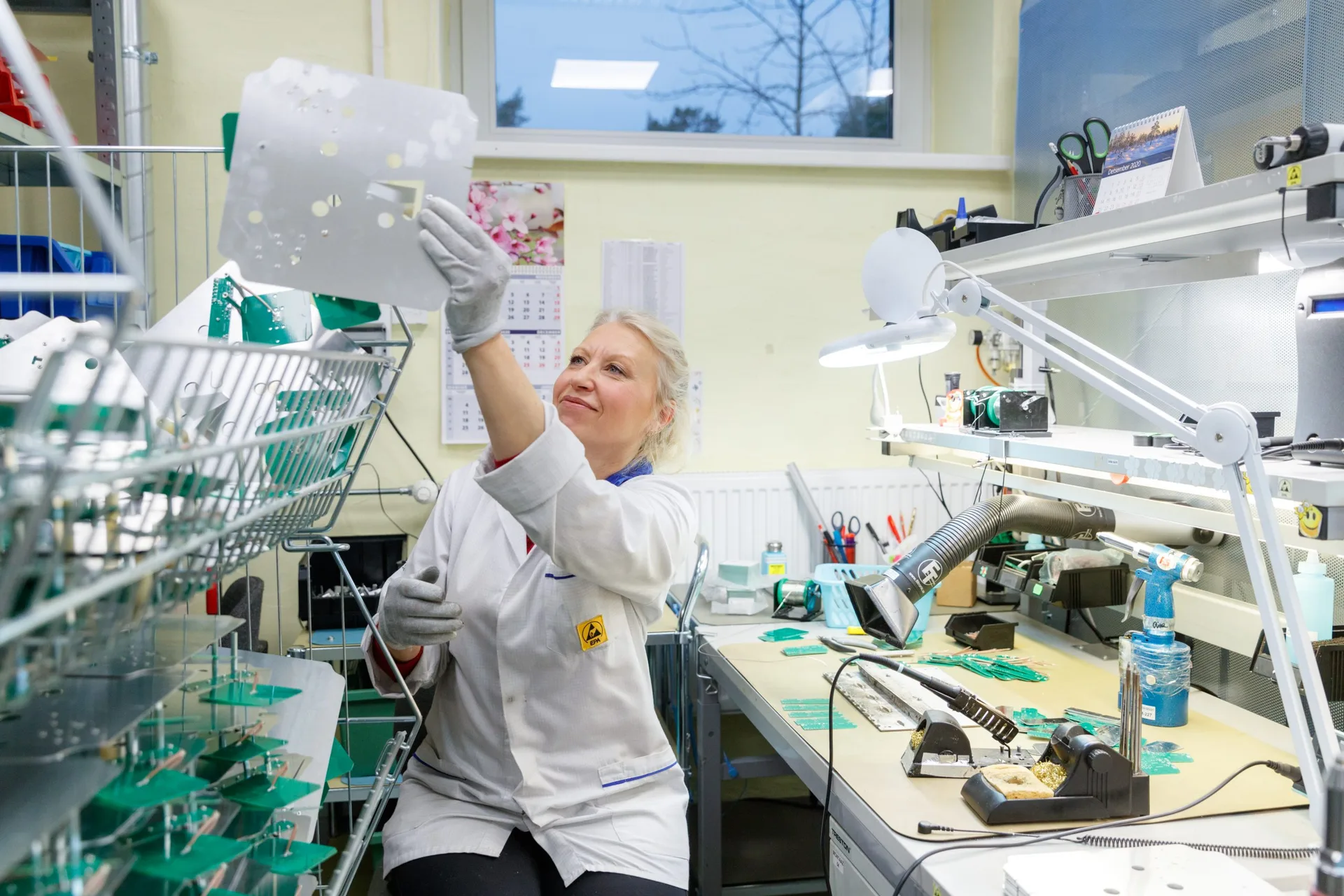
From circuit board to working product. PCB assembly, inspection and testing, with design, tuning and repair support. Choose a single production stage or a complete manufacturing service.
Discuss your projectWhat we do
Electronic device design and PCB layout, with RF engineering expertise.
Automated SMT production, selective through-hole soldering and hand assembly.
Automated optical inspection, functional testing, RF tuning and repairs.
All production takes place at Rantelon in Tallinn, Estonia, within the European Union. We keep your designs, production files and technical information confidential throughout the process.
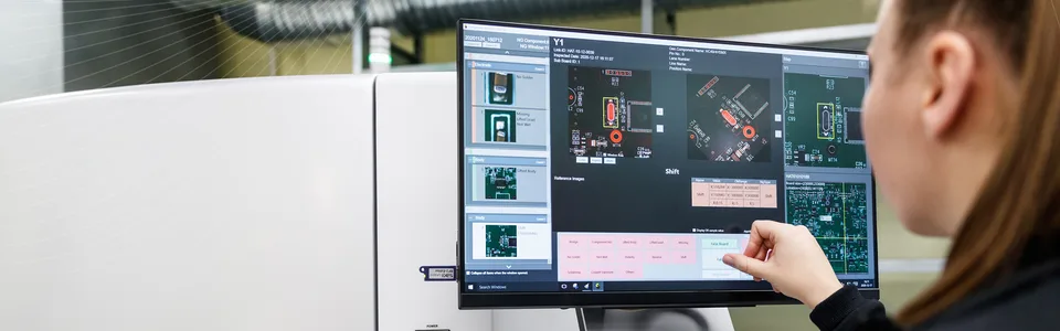
Inside production
Components are handled in a controlled environment. Assemblers receive IPC training, supported by an ISO-based management system.
Start a project